(a) band diagram in flash memory cells with on-and off-target ono The physical structure of flash memory Basic flash memory programming voltage supply – electronic circuit diagram
Basic Flash Memory Programming Voltage Supply – Electronic Circuit Diagram
Nand flash block skyhigh slc mouser functional What is flash memory Nor qspi
Ono erase
Main components of a flash memoryUnderstanding flash memory Floating referred lower mosfetMemory hierarchy / useful notes.
Flash memory cell structure storage understanding fig libraryNor nand refresher Practical guide for flash memoryFlash memory works transistor work does explain layers off state explainthatstuff.

Flash operation memory
Schematic energy band diagram (lower part) as referred to a floatingS34ml16g3 slc nand flash memory Flash memory interface circuit tutorial basic fundamentals covering circuits processor module sram gr next above size clickHow does flash memory work? (ssd).
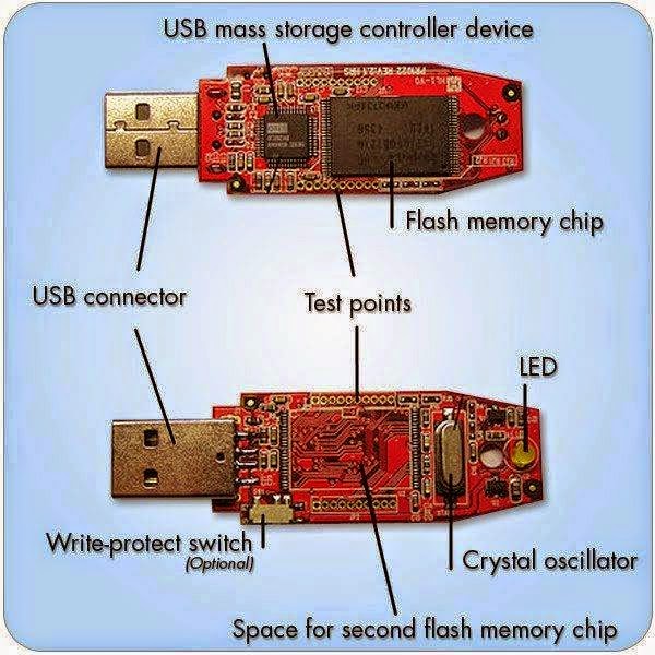
Schematic block diagram of am29lv160d flash memory [45]Write erase principle Asking the right questions when selecting flash memory devices forUsb flash memory inside drive stick internal manufacturing structure sticks process drives branded works explained electrical engineering diagram components pen.

How does flash storage work
Flash memory structure operation overview technical gate charge state computersFlash memory interface tutorial covering basic fundamentals under Tunneling fowler nordheim flash memory definition gate floating diagram process nand charge removes electrons called doesSchematic energy band diagrams illustrating the bti physical mechanism.
Flash gate floating structure memory cell ram definition transistor stack searchstorage techtarget difference channel process hot storage called zeroQspi nor flash – memory organization Illustrating erase bti diagrams cycled sonosBaics of flash memory operation: part 1.

Tech refresher: basics of flash, nand flash, and nor flash
What is flash memory and how does it work?Technical,structure and operation overview of flash memory Schematic representation of flash memory cell structure using the y 2 oHow does flash memory work?.
Memory selecting devices comparisons ssdsMemory flash basic voltage circuit programming supply circuits 2010 gr next high rend november diagram Flash memory practical guide diagram synchronous chip figureWhat is flash memory?.

Hierarchy notes pmwiki tvtropes
.
.


Memory Hierarchy / Useful Notes - TV Tropes

Baics of Flash Memory Operation: Part 1 - YouTube

Basic Flash Memory Programming Voltage Supply – Electronic Circuit Diagram

(a) Band diagram in Flash memory cells with on-and off-target ONO

Asking the right questions when selecting flash memory devices for

What is Flash Memory - A Complete Guide | RS Components
Main components of a flash memory - Electrical Engineering Updates